-JFET (junction gate field effect
transistor) that kind of transistor that’s main difference from the BJT (bi-polar
transistor) is that BJT can be considered as current control devices (dependent
current source) while the JFET can be considered as voltage control device.
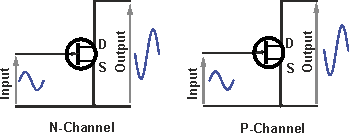
There are two types of JFET, the p-type JFET that consists of a middle channel of a semiconductor material having large number of positively charges carriers, while the N-type JFET that consists of a middle channel of a semiconductor material of negatively charged carriers.
Through this transistor the Electric charge passes through the channel from the source pole to the drain pole along the channel.

So in this transistor as we apply some voltages at its terminals, VGS = 0 v, VDS = +ve voltage.
So at the channel which is N-type the electrons will be attracted to the drain which we apply a positive voltage at it, at the gate terminal which is P-type, by the applied voltages here we noticed that the p-type forms with the n-type a reverse bias which makes the depletion region larger and by increasing the drain source voltage VDS the depletion region larges until it reaches a critical point where approximately no electric field can pass from the source to drain and that makes the resistivity of the device increase, this voltage is called the pinch-off voltage VP, a small current can pass through the channel that us highly attracted to the drain terminal which called the saturation current IDSS that passes through the channel when applying VDS ≥ VP after exciding the pinch off voltage , the current will stay constant which will be IDSS and its physical formula can be given by :
ID = IDSS (1-VGS/VP)^2

There are three
types of connecting a JFET in a Circuit to do a certain function.
a.Common gate
This configuration
provides a low input impedance while provides a high output impedance, although
the voltage is high, but the current gain as well as the power gain are low,
there is an advantage in this configuration is that the input and the output are
in phase.

b. Common drain
This configuration is known as source follower, as
the source voltage follows the gate input voltage, that offers high input
impedance and low output impedance, it is used as a buffer just to separate the
input from the output,
The voltage gain here is one, the input voltage and the output one seems to have the same voltage, although the current gain is high, and the input and the output signals are in phase.
The voltage gain here is one, the input voltage and the output one seems to have the same voltage, although the current gain is high, and the input and the output signals are in phase.

c.Common Source
This configuration
is the most widely used as the common source circuit in general provides a
medium input and output impedance, and both current and voltage gains can be
described as medium, but the output signal is shifted by 180 degree (the out is
the inverse of the input signal).
you are clear my mind actually after reading your article i got clear my complete doubt. thanks for such easy understanding post. Sharing on what is pinch off voltage for a jfet for future aspect at here http:// electrotopic.com/what-is-the-pinch-off-voltage-for-a-jfet/
ReplyDelete